

The CA16 addresses key challenges in the bump inspection of flip chips and wafers. Through 2D and 2.5D X-ray imaging combined with AI-powered automatic image analysis and metrology, the system identifies critical defects with submicron precision. With inline capability and direct process feedback, the CA16 increases yield, and accelerates time-to-market
Highlights
- Focus on 2.5D acquisition ensures fast scan time
- Available with fully automated operation for seamless integration into your fab
- AI-based data analysis and advanced software ensures fast, accurate defect classification to resolve systematic issues and maximize yield
- Non-destructive technology for insights into solder bumps or TSVs within seconds
- Repeatable results through reliable and accurate technology, designed to support a stable inspection routine
Key benefits
 | Easy to use.→ Fast insights on critical defects. | |
 | Reliable quality and process assurance.→ Ship zero-defect products. | |
 | AI-based data analysis.→ Resolve systematic issues, maximise yield. | |
 | Monitor process implementation.→ Faster time-to-market. |
From lab to fab.
Whether you need the highest quality images to inspect your parts in a Lab/R&D environment, or you require a fully-automated solution that easily fits into your existing production process, the CA16 is available in a variety of configurations to suit your needs.
MXI applications
The CA16 MXI/Lab configuration is designed to provide fast, high resolution images of single layer bumps for manual inspection, for example C4 bumps and BGA's. For the fastest scan time, 2D X-ray provides rapid results, while 2.5D X-ray captures images at a tilted angle to provide additional depth information.


AXI applications
With the addition of an EFEM loader for 300mm wafers, and our AI-powered software packages for automatic image analysis and metrology, the CA16 in AXI/Fab configuration automaitcally identifies and measures defects in both bumps and TSVs and feeds these insights back directly into your processes for improvement.

AI-powered metrology clearly identifies and measures voids in a 2D X-ray image of a wafer with solder bumps (50 μm – 30 μm single layer)*.
*Test parts designed for Comet by Fraunhofer IZM-ASSID, they contain defects for illustrative purposes
- Real time inspection powered by our AI driven ADC software CoW Insights X 2D
- User friendly recipe set-up, including simple configuration of production limits, easy test and validation and import/export between systems
- Information can be extracted into machine readable formats for post data processing and reporting (e.g. KLARF, json, xml)
- Supports faster, data-driven decision
making for rapid process feedback
 Before segmentation
After segmentation
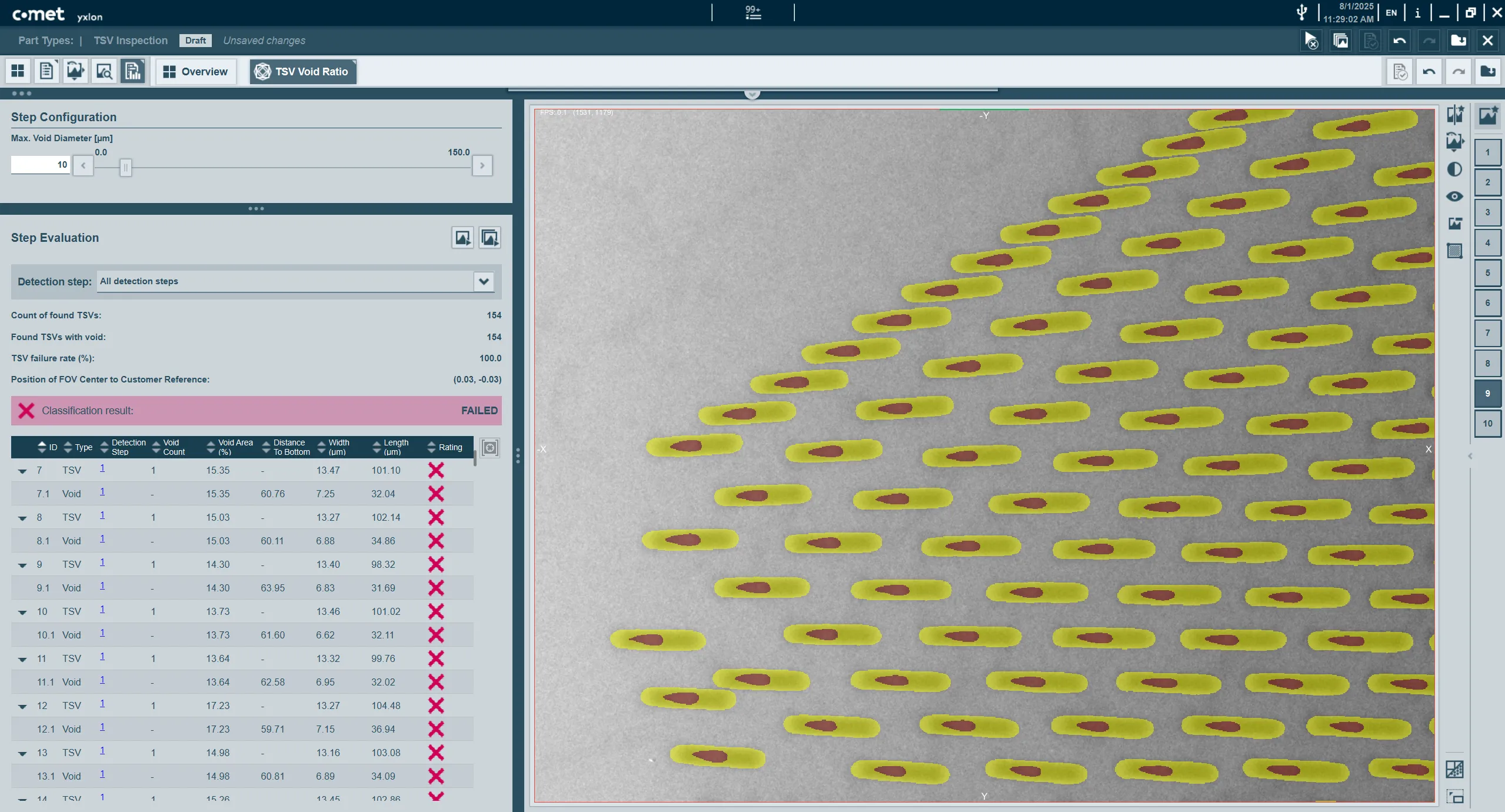
Screenshot taken from our TSV Insights X 2.5D software. Image shows a wafer sample (source: Fraunhofer IZM-ASSID) where all TSVs have been manipulated to contain voids. The image shows the segmentation of each TSV (yellow) and the voids within (red).
Software Solutions
From software tools that rapidly detect and analyze the size and severity of defects, such as voids and bridges, to solutions that ensure delicate components remain shielded from harmful X-rays, the CA16 is equipped with a range of advanced software solutions across our three pillars of Clarity, Efficiency and Insights. Explore just a few of these below.

1. Clarity
Image acquisition
Gain highest image data quality: See more details of your inspection samples by capturing brilliant 2D and 2.5D images.
Clarity Packages
Our Clarity Packages for 2D and 2.5D image aquisition are tailor-made for inspection with the CA16 system. Due to the precise manipulation of the CA16, its dedicated semi X-ray imaging chain and the powerful 2D volume reconstruction software, they allow for excellent resolution and capture of the finest details.
Explore our entire software suite

2. Efficency - Connectivity & management
Increase your productivity: Streamline workflows between systems, software and people through seamless connectivity and automation.
Dose Manager
The Dose Manager package continuously monitors and tracks the X-ray dose that the sample is subjected to, taking into account the tube power and the distance to the sample. To avoid damage to sensitive components such as flash and DRAM memories, it switches off the X-ray automatically once the dosage limit is reached. The package includes a Dose Reduction Kit with a collimator and 4 filters, shielding parts outside the region of interest from radiation.
Explore our entire software suite
Batch Manager / Wafer Manager
Loading multiple parts at the same time by using a multi-part holder can significantly increase your throughput. The Batch Manager package allows you to automatically inspect parts in a grid by applying the same inspection sequence in a grid of a multi-part holder. Deviations of the sample positioning are corrected without user interaction.
For wafer inspection applications, our newly released Wafer Manager package automatically aligns wafers for inspection in seconds. Users can define the wafer map manually, or use our intuitive wizard. With the wafe rmap, you can quickly select the relevant dies for your inspection and the system will perform the same inspection task on each to standardize your inspection process.

3. Insights - Image analysis & process control
Improve product and process quality: Extract critical information from image data to stay ahead of your market.
CoW Insights X 2D*
CoW Insights X 2D is our specialised software for the CA16 equipped with a fully-automated inspection package specifically designed for wafer level packaging. It provides fast, sufficient quality 2D image acquisition, and ensures early defect detection and process control for fine-pitch micro bumps down to 20μm on wafers
- Accurately extract bump and void measurement using automated 2D images analysis solution
- Maintain high inspection throughput and precision with reliable automated defect recognition powered by Dragonfly AI technology
- Enable real-time process control and inline monitoring with actionable 2D metrology data
- Maximize yield with accurate and repeatable quantitative inspection results
- Results visualization for root cause analysis and for inspection recipe validation
- Data available in machine readable formats for statistical analysis and post processing
- Review Insights included
*CoW Insights X 2D is available in combination with the automatic loader
Explore our entire software suite
TSV Insights X 2.5D*
TSV Insights X 2.5D is our specialised software for the CA20 equipped with a fully-automated inspection package specifically designed for wafer level packaging. It provides fast, sufficient quality 2.5D image acquisition, and fully automated TSV metrology and defect classification including reporting for automated processing.
- Speed up time to market and time to volume with real-time feedback, and ship zero defects by identifying critical defects early
- Improve yield by process control based on accurate and reliable automated TSV metrology information and increase productivity due to full integration into your production chain
- Extracted information is also available in machine readable form for post reporting jobs, e.g. KLARF, json, xml and direct access reports can be automatically transferred to your preferred local storage location
*TSV Insights X 2.5D is available in combination with the automatic loader
Explore our entire software suite
Dragonfly 3D World
Analyze your 3D X-ray data with this intuitive image processing software suite. Utilize the power of AI and use the deep learning segmentation to extract the maximum of information from the low dose scan that protects sensitive components. If you do not need the numbers, simply highlight your results with stunning visuals.

CA16 inspection applications in R&D and production
- Chip-on-Wafer (C4 bumps and copper pillars)
- 2.5 IC package solder connections including microbumps
- TSV inspection
- Flip-Chip inspection
- Substrate strip solder bumps
- Sensors
- MEMS and MOEMS

A 2.5D X-ray image of a flip chip, with voids in bumps segmented and visible in red. *Test parts designed for Comet by Fraunhofer IZM-ASSID, they contain defects for illustrative purposes
See more of CA16 in the gallery:


50µm solder bumps on wafer scanned using CA16 in 2D X-ray mode, test part from Fraunhofer IZM-ASSID


Your download:
 CA16 Flyer (English) (pdf)
Register to download
Technical Data
Application/Version | MXI / Lab | AXI / Fab |
| Max. inspection envelope | Ø 435 mm (17’’) or | Ø 300 mm wafer mount |
| System Dimensions (W/D/H) | 1,770 mm × 1,400 mm × 2,050 mm | 1,860 mm × 2,700 mm × 2,300 mm |
| Max. Part Weight | 0.5kg | 0.5kg |
| Detector Active Area | 130 x 130 mm | |
| Pixel Matrix | 1536 x 1536 px | |
| Pixel Pitch | 85 µm | |
| Manipulation - tilt angle | +/- 65° (130°) | |
| Scan Modes | 2D, 2.5D | |