

Date
10 - 13. November
Location
Munich Messe,
Munich, Germany
Booth
Hall B1, Booth 572
SEMICON Europa is just around the corner, and as one of the highlights of our event calendar, we can't wait to welcome you to Booth #572 in Hall B1. Over the years, SEMICON Europa has been the stage for some of our biggest semiconductor milestones, from the launch of our advanced packaging inspection specialist, CA20, in 2023, to fully automated semiconductor inspection in 2024, and the expansion of our portfolio with wafer inspection solutions in 2025. And this year will be no exception. Join us in Munich to discover the latest additions to our semiconductor portfolio and get a glimpse into the future.
X-ray for semiconductors:
What makes it a game-changer?
2.5D and 3D X-ray inspection bridge the gap between speed and visibility – giving semiconductor manufacturers unprecedented insight into the internal health of devices without destructive methods. But how do these technologies work?
2.5D X-ray
2.5D X-ray combines multiple-angled images to give depth-like information (a “pseudo-3D” view). By offering better depth discrimination without the full computational cost of 3D, it is ideal for inline inspection where speed matters.
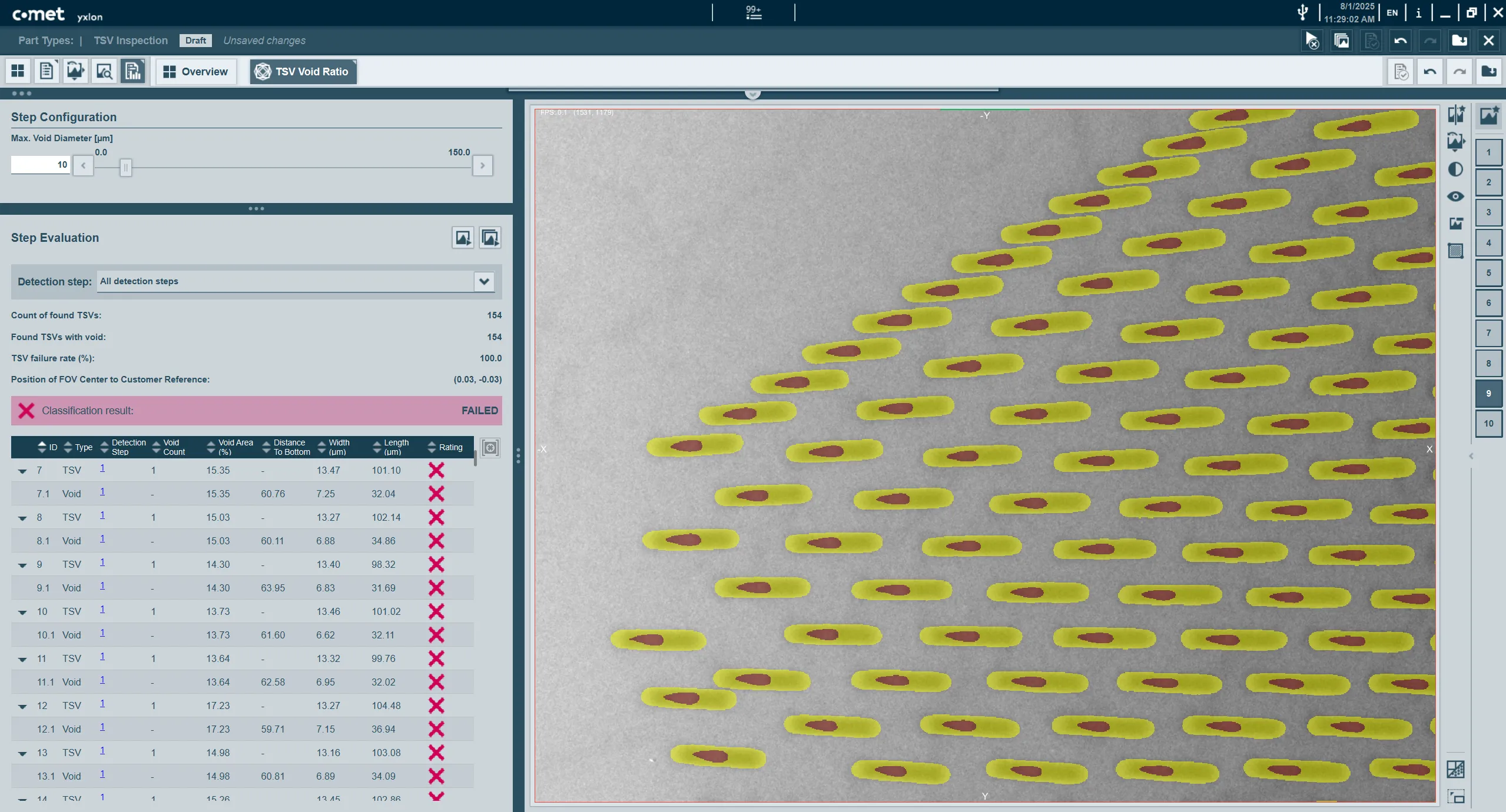
Screenshot taken from our TSV Insights X 2.5D software. Image shows a wafer sample (source: Fraunhofer IZM-ASSID) where all TSVs have been manipulated to contain voids. The image shows the segmentation of eachTSV (yellow) and the voids within (red).
3D X-ray (CT)
3D X-ray (CT or computed tomography) reconstructs a true volumetric image of the sample. It allows engineers to slice through the component virtually and inspect each layer, revealing hidden internal features with high precision – essential for advanced packaging and failure analysis.

3D X-ray image of micro-bumps within a CPU. Captured by the CA20 and rendered in Dragonfly 3D World.
Get to know our product range

CA20
Now available as a fully-automated inspection solution for Advanced Packaging, the CA20 is designed to deliver superior 2D & 3D images in the highest resolution, and helping identify structural defects in solder bumps and TSVs fast.

FF35 CT
With its optional dual-tube set-up, the FF35 CT combines unprecedented CT data quality with the highest versatility, particularly in lab environments. With specific variants developed specially for inspections in semiconductor-related industries, the FF35 CT SEMI is certified to the industry standards SEMI® S2-0818 & SEMI® S8-0218

Cheetah EVO & Cougar EVO
High detail resolution and very flexible X-ray systems for 2D/2.5 D, 3D laminography
and computed tomography imaging. For R&D and at-line inspection in traditional packaging
environments. Our Cheetah EVO Semi is SEMI® S2-0818 & SEMI® S8-0218 certified
Want to experience the Cheetah EVO live?
Just across the hall at the electronica, you can also get to know our reliable, and advanced system for electronic component inspect at the booth of our partner ATEcare.
Hall A4, Booth #346
Don't have your ticket yet?
Our team still has a few free tickets available exclusively to our customers (present and future). If you would like to request a free ticket for both the semicon europa and the electronica, please fill out the form below and our team will reach out to you.